Printers circuit boards (PCB) are one of the most important parts of any electronic device. Calculators, watches, DVD players, computers and cell phones all including a basic PCB. Printed circuit board is an electronic circuit that is mounted on a board of non -conducting material and the electronic components on the board are conducted by creating conducting channels. It comes in three basic varieties, single-sided, two-sided, and multi-layered.
PCB Fabrication
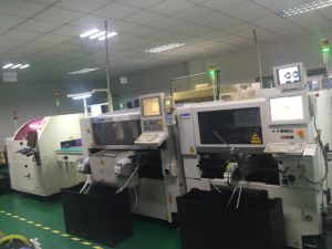
When you move ahead with the printed circuit board fabrication in China process, you must know that it’s a difficult and very critical series of operations. The first step of the PCB fabrication process includes the transfer of schematic from to the real time capture. When the schematic is entered, the PCB fabrication process is used to place the parts on the single PCB board. When layout gets completed the board layers are fully printed onto toner transfer paper. The image is then transferred to the bare copper board with a highly advanced laminating machine. After lamination, the paper board is removed with the paper and leaving the toner behind.
At the very first step, outlines are made on the boards and then connectors are marked on a white and smooth sheet of paper. This step is then followed by the sketching of the component outlines with connecting point and other comprehensive conductor patterns. Engineers view the PCB layout from the component side first to ensure no illusion through the fabrication. Among all the components on the PCBs, larger components are filled first. You should place the right PCB angles with minimum spacing requirement.
Etching is very important fabrication process that is formed by the selective removal of copper around the boards. A copper solution is highly useful etching solution that’s made into a solution of water into the marked copper clad. If you want to have unpopulated circuit boards in the PCBs, you should check the circuit connections to verify the connection on finished circuit board. In a situation where high volume circuit board productions are done, engineers use a bed of nails tester to make contact with the components of perfect copper. Engineers use computers to control the electrical testing unit. This testing unit is used to communicate and send a small current through every contact point. These contact points are verified on the basis of appropriate contact points instituted on PC boards.
On the outer surface of the circuit board, several component designers are installed by the manufacturers to ensure that the entire PCB fabrication process completes in the finest manner possible. While choosing service providers for the PCB fabrication process, one should ensure to go ahead with a provider that offers the fabrication services in strict compliance and compliance with the industry standards. These services are offered precisely and in very affordable manner to the global customers.
Printed Circuit Boards fabrication process includes very complex and difficult phase of operations. Several component designators are installed by the manufacturers to ensure that the entire PCB fabrication process completes in the finest manner possible.